Silicon photomultipliers will provide a core enabling technology in the Cherenkov Telescope Array, the world’s largest and most sensitive gamma-ray observatory

Hamamatsu Photonics, a Japanese optoelectronics manufacturer that operates across diverse industrial, scientific and medical markets, is evaluating cutting-edge opportunities in high-energy physics for its silicon photomultiplier (SiPM) technology portfolio. Near term, that means the focus is on emerging applications in astroparticle physics and gamma-ray astronomy, while further down the line there’s the promise of at-scale SiPM deployment within particle accelerator facilities like CERN, KEK and Fermilab to probe new physics beyond the Standard Model.
What of the basics? The SiPM – also known as a Multi-Pixel Photon Counter (MPPC) – is a solid-state photomultiplier comprised of a high-density matrix of avalanche photodiodes operating in Geiger mode (such that a single electron–hole pair generated by absorption of a photon can trigger a strong “avalanche” effect). In this way, the technology provides the basis of an optical sensing platform that’s ideally suited to single-photon counting and other ultralow-light applications at wavelengths ranging from the vacuum-ultraviolet through the visible to the near-infrared.
Hamamatsu, for its part, currently supplies commercial SiPM solutions into a range of established and emerging applications spanning academic research (e.g. quantum computing and quantum communication experiments); nuclear medicine (e.g. positron emission tomography); hygiene monitoring in food production facilities; as well as light detection and ranging (LiDAR) systems for autonomous vehicles. Other customers include instrumentation OEMs specializing in areas such as fluorescence microscopy and scanning laser ophthalmoscopy. Taken together, what underpins these diverse use-cases is the SiPM’s unique specification sheet, combining high photon detection efficiency (PDE) with ruggedness, resistance to excess light and immunity to magnetic fields.
Gamma-ray insights
Evidently, those same characteristics are well-matched to the technical requirements of the next generation of detectors for astroparticle physics (the study of elementary particles of cosmic origin and their relation to astrophysics and cosmology). A case in point is the Cherenkov Telescope Array (CTA) Observatory, an ambitious international research initiative that’s in the process of building the world’s largest and most sensitive high-energy gamma-ray observatory, comprising 64 telescopes of different sizes to cover a broad gamma-ray energy range (from 20 GeV to 300 TeV). The telescopes will populate two arrays – one site located in the Canary Islands, Spain; the other in Chile – to cover both the northern and southern hemispheres.

By way of context, when gamma rays reach the Earth’s atmosphere, they interact with its outer layers to produce cascades of subatomic particles known as “air showers” or “particle showers.” These ultrahigh-energy particles can travel faster than light in the air, creating a blue flash of Cherenkov light (like the sonic boom created by an aircraft exceeding the speed of sound).
While spread over a large area (typically 250 m in diameter), the Cherenkov light lasts for only a few nanoseconds – just long enough to be tracked by the mirrors of the CTA’s telescopes and detected by the high-speed cameras positioned at their foci. As such, the CTA will ultimately enable astronomers to investigate the parent gamma rays and their cosmic origins.
“In terms of ongoing product development and innovation, we are interested in how the SiPM platform can be used for atmospheric detection of Cherenkov light,” explains Mauro Bombonati, senior sales engineer at Hamamatsu Photonics’ Italian division in Milan. “We see the CTA initiative as an ideal proving ground for advanced SiPM detectors and, by extension, a stepping-stone for future deployment of SiPM technology in large-scale accelerator facilities – for example, to support neutrino experiments and the search for dark matter.”
Blue-sky collaboration
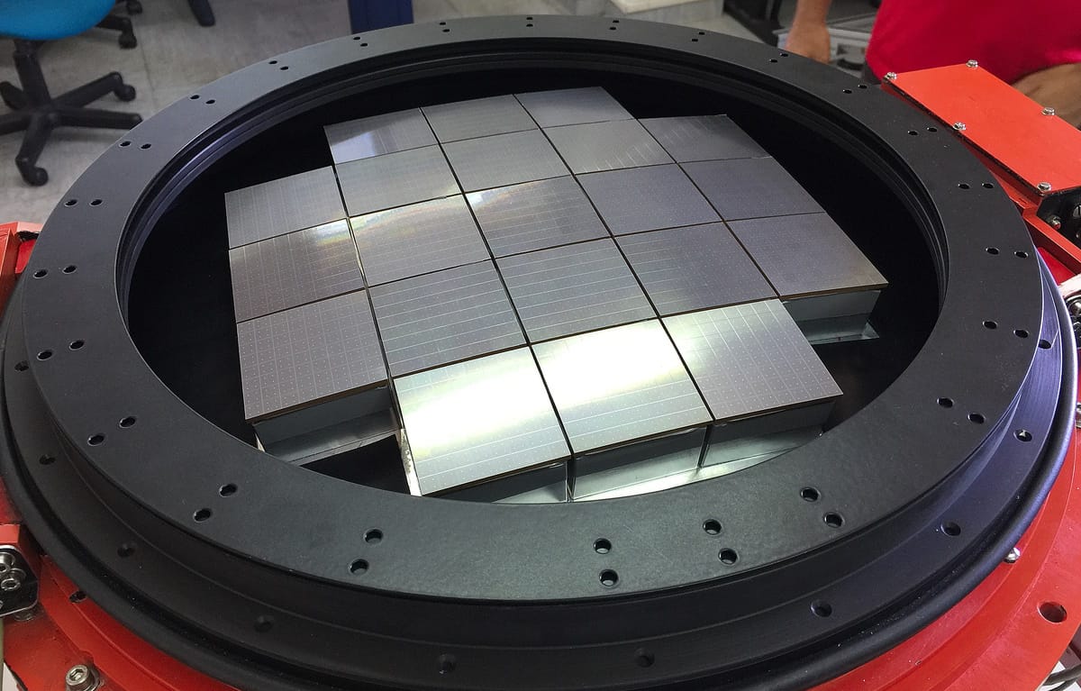
With this in mind, Hamamatsu’s R&D team has collaborated closely with the Italian National Institute of Astrophysics (INAF) in the context of the ASTRI project, an international consortium that’s in the process of building nine dual-mirror telescopes (4 m in diameter) for atmospheric Cherenkov astronomy. As a preferred technology partner, Hamamatsu handled the design, development and optimization of ad hoc SiPM modules used to populate the compact Cherenkov cameras of the ASTRI telescopes. The resulting ASTRI mini-array is currently being installed at the Teide Observatory (Tenerife, Canary Islands) and represents a “pathfinder” for the CTA’s sub-array of 37 small-scale telescopes (SSTs) that will be installed at Paranal (Chile).
Upon completion, the CTA will further comprise 23 medium-sized telescopes (MSTs) – each at 12 m diameter and distributed over both array sites – as well as four large-sized telescopes (LSTs) at 23 m diameter. Operationally, the LST and MST camera systems will exploit photomultiplier tubes; the SST cameras, in contrast, will use SiPMs to convert Cherenkov light into electrical data for high-speed readout and analysis.
It’s also worth noting that INAF, along with other CTA project teams, is pursuing variations on the SST theme, with slight modifications to the geometry and design of the SST telescopes to realize an optimum approach versus CTA technical requirements. Within Hamamatsu, too, the device-level R&D effort is ongoing – specifically improving SiPM PDE in the near-UV (200–400 nm), where Cherenkov light intensity is optimum.
“We’re improving the wafer fabrication process to reduce the number of lattice defects in the photoelectric conversion layer,” notes Bombonati. The goal is increased carrier lifetime and greater numbers of carriers reaching the avalanche layer. “To date,” he adds, “Hamamatsu engineers have demonstrated a 16% enhancement in the detector sensitivity at 350 nm.”
Another focus of Hamamatsu’s R&D involves pile-up suppression in SiPM detectors – i.e. to make the rising edge of the signal waveform sharper by adjusting the quenching resistor and reducing terminal capacitance. In this way, a lower trigger threshold can be used to separate Cherenkov “events” from noise, such that lower-energy events can be observed as standard.
Equally significant is the exploitation of through-silicon-via (TSV) technology, which is essentially a vertical electrical connection that passes completely through a silicon wafer to maximize the active area for photon detection while simultaneously minimizing dead space (thereby enhancing PDE while also lowering crosstalk between SiPM pixels).
Competitive intelligence
Strategically, Hamamatsu maintains a watching brief on the wider landscape in high-energy physics to ensure a customer-driven frame of reference for its in-house innovation programme. A case in point is the company’s “observer status” within CERN’s European Committee for Future Accelerators (ECFA), an initiative that underpins community-wide development of long-term R&D roadmaps for accelerator and detector technologies.
“Engagement with the ECFA helps us to prioritize emerging technology trends and user requirements for SiPM in astroparticle physics and accelerator-based science,” concludes Bombonati. “At the same time, developing SiPM solutions for frontier research in high-energy physics also yields paybacks elsewhere – not least in terms of enhanced capability and competitive differentiation for our more established industrial applications.”
- SEO Powered Content & PR Distribution. Get Amplified Today.
- PlatoAiStream. Web3 Data Intelligence. Knowledge Amplified. Access Here.
- Minting the Future w Adryenn Ashley. Access Here.
- Buy and Sell Shares in PRE-IPO Companies with PREIPO®. Access Here.
- Source: https://physicsworld.com/a/silicon-photomultipliers-gearing-up-for-applications-in-gamma-ray-astronomy/